Table Of Content
If you need a PCB design tutorial to help you get up to speed quickly, you’ll have access to a variety of resources you need to be successful. The resources listed below contain PCB routing tutorials, guides on how to use PCB design tools, and much more. Anyone can access Altium’s knowledge base, blogs, webinars, and more for free.
New circuit boards can be repeatedly recycled
These lights use a printed circuit board (PCB) to control the timing and sequencing of the lights. The PCB layout is a crucial part of the traffic light system, as it determines the accuracy and reliability of the signals. IEC Electronics Corp.Located in Newark, NY, IEC Electronics Corp. has 740 employees.
PCB Design Software industry growth trends illuminated by new report - WhaTech
PCB Design Software industry growth trends illuminated by new report.
Posted: Tue, 12 Mar 2024 07:00:00 GMT [source]
Assembly Capabilities
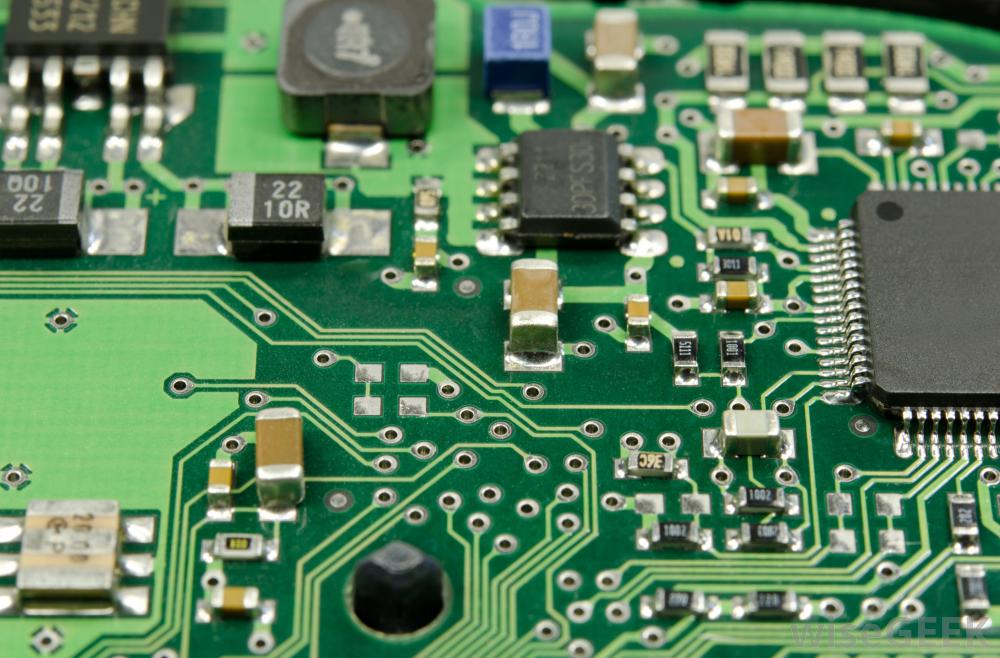
Did you know that you can use vias to move heat from one side of your PCB to the other? This can come in handy when you need to lower the operating temperature of your components by pushing some heat to the other side of your board. It would be best if you had considered the component placement necessary during the design phase.
PCB Board Design: The Ultimate Guide to Great Printed Circuit Board Layout
The layout includes electronic components such as microcontrollers, sensors, and relays that work together to ensure the lights operate as intended. Some professionally made circuit boards use a different method to remove extra copper from the circuit board. Resist is an ink that resists the etchant used to make the circuit board.
Schematic Design
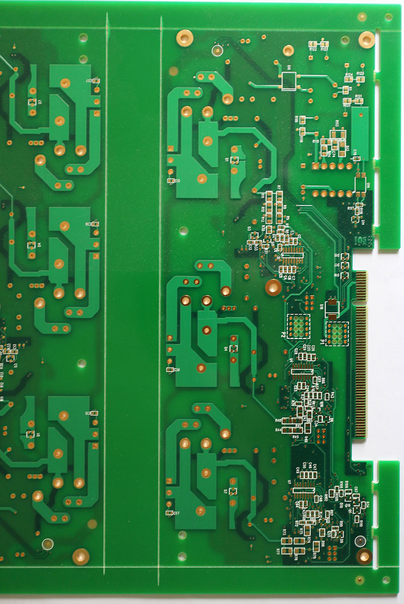
These planes also do the important job of returning the signals that are routed with traces. If the planes have too many holes, cut-outs, or splits, it can cause these return paths to create a lot of noise and degrade the performance of the PCB. There are multiple additional aids available to the designer, such as design grids that can help to place components and route traces in a neat and orderly manner.
Step 3: PCB Design – Your Board Layout
The vitrimer jelly can then be repeatedly used to make new, high-quality PCBs, unlike conventional plastics that degrade significantly with each recycling. With these "vPCBs" (vitrimer printed circuit boards), researchers recovered 98% of the vitrimer and 100% of the glass fiber, as well as 91% of the solvent used for recycling. Damaged circuit boards, such those with cracks or warping, can in some cases be repaired. If they aren’t repaired, they can be separated from their electronic components. With these “vPCBs” (vitrimer printed circuit boards), researchers recovered 98% of the vitrimer and 100% of the glass fiber, as well as 91% of the solvent used for recycling. Traffic lights are essential to keep traffic flowing smoothly and prevent accidents on the road.
That plastic can’t easily be separated from the glass, so PCBs often pile up in landfills, where their chemicals can seep into the environment. Or they’re burned to extract their electronics’ valuable metals like gold and copper. This burning, often undertaken in developing nations, is wasteful and can be toxic — especially for those doing the work without proper protections.
It helps manufacturers and designers to understand the capabilities and limitations of a PCB, ensuring that it meets the specific requirements of a particular application. The Board Class is determined by various factors, including the materials used, the manufacturing processes employed, and the level of testing and inspection performed. These factors collectively determine the overall quality and performance of the PCB. There are several different Board Classes, each with its own set of requirements and specifications. PCB circuit board design tools must have the features and functionality required for creating complex designs.
"Moving forward, we need to design and optimize materials with sustainability metrics as a first principle." Or they're burned to extract their electronics' valuable metals like gold and copper. This burning, often undertaken in developing nations, is wasteful and can be toxic—especially for those doing the work without proper protections. Z.Z., J.A.S. and B.H.N. designed the repair experiments and evaluations.
Components should be placed in a logical and organized manner, with consideration given to factors such as signal integrity, thermal management, and manufacturability. Once the PCB layout is complete, the design undergoes a series of verification and validation steps, including design rule checks (DRC), electrical rule checks (ERC), and signal integrity simulations. These steps help identify and resolve any potential issues before the design is sent for manufacturing. Part two will focus on translating PCB design into reality, exploring the intricacies of PCB manufacturing, assembly, testing, and debugging. Finally, we'll navigate the industry's leading PCB design software and tools, setting the path to creating high-performance electronic devices.
Renesas to acquire Altium for $9.1 billion - Business News Australia
Renesas to acquire Altium for $9.1 billion.
Posted: Thu, 15 Feb 2024 08:00:00 GMT [source]
The silk screen is used to add information to the PCB that allows it to assemble more easily and be better understood by humans. Usually this information takes the form of numbers, letters and other symbols, such as function notations for the pins or LEDs. Umar is an electrical engineering graduate with a strong technical background in Robotics, IoT, Industrial Process and Control, Embedded Systems, Power Electronics, and Electronic Network Analysis. In addition to his electronic troubleshooting expertise, he has a passion for writing and consistently... This makes it a huge pain to keep the width of your traces consistent, especially as they get narrower.
The components are soldered onto the board, creating an electrical pathway for transmitting signals and power. DRC and DFM are two critical aspects of the PCB design workflow that help ensure the integrity and manufacturability of the printed circuit board. Schematic design is a critical step in the PCB design workflow, as it lays the foundation for the entire project.
A. Crosstalk can be minimized by proper trace routing (e.g., avoiding parallel runs, using guard traces), ground plane placement, and the use of differential signaling. Simulation tools can also be used to identify and mitigate crosstalk issues. By carefully considering these factors and following best practices for signal integrity and EMC, designers can create PCBs that perform reliably and meet the required regulatory standards. By following DRC and DFM guidelines, designers can create PCB layouts that are both functional and manufacturable, reducing the risk of manufacturing issues and ensuring a high-quality end product.
There are also flexible PCBs built on flexible high-temperature plastic (Kapton or the equivalent). Once you have set up your CAD tool, it's important to familiarize yourself with its features and functionalities. Most CAD tools offer comprehensive documentation and tutorials to help you get started. Take advantage of these resources to learn the ins and outs of the software. Additionally, online communities and forums can be valuable sources of support and knowledge.


No comments:
Post a Comment